Master Switch Electronics
In my first year on Longhorn Racing Electric (UT Austin's Formula SAE electric car team), I was tasked with designing and assembling the Master Switch PCB. The PCB interfaces with the car's main switches that enable the low voltage and high voltage systems.
One of the core requirements for the design was that it allowed for the low voltage battery to be bypassed by an external source for trackside maintenance and debugging without having to drain the car's battery. It also needed to be possible to charge the low voltage battery without removing it from the car.

I met this requirement by selecting a DPDT switch that allowed for simultaneous use of an external bypass battery and charging of the car's battery. I also made sure that the component was rated for the current of the entire LV system, which is mainly for cooling (up to 25A).
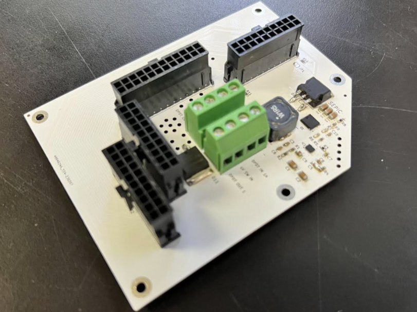
I also had to lay out a SEPIC (single-ended primary-inductor converter) to drop the 24-26V LV battery voltage to a stable 12V for interfacing with some off-the-shelf 12V components, like our BMS.
We chose a SEPIC over a simpler buck topology because our bypass battery was planned to be a 12V lead-acid battery, so it needed to be able to pass through a 12V input to a 12V output without a significant drop.

Above is my attempt at laying out the SEPIC. It worked, but on the oscilloscope, I observed that the output voltage would spike to about 13V at the SEPIC IC's switching frequency because I failed to account for the parasitic inductance of the switching loop.
I had learned about parasitics pretty late in the season, but below are a couple alternative layouts that drastically reduce the switching loop's area, reducing parasitic inductance and the resulting voltage spikes.

For high-current paths, I used copper fills on both sides that were connected with vias. I estimated the necessary width of these fills from the definition of resistance and by choosing an acceptable voltage drop and temperature delta. The resulting heating ended up being acceptable during testing.

My PCB also had to pass through a lot of signals like CAN lines and other digital signals, so I made sure the signals were above a ground plane to mitigate EMI.

A few days after I ordered the PCB, its bounding box requirements changed due to a domino effect from a mechanical change, so I had to use a dremel to remove a part of my PCB that served as a redundancy, the HV measurement points.

To make matters worse, I also had the wrong footprint for the SEPIC's inductor. Pictured below is my attempt to work around this issue, but at this point my team lead told me it was time for a second revision.

I respun the board by making it conform to the new dimension requirements and fixing that one footprint.
After assembling the PCB, it was time to harness it within the enclosure that a mechanical engineer designed. Because the enclosure had to be watertight, I had to internally harness wires from the PCB to bulkhead connectors on the enclosure walls, and externally harness wires between enclosures.

Here's a photo of the finished Master Switch enclosure.

Finally, here's a picture of the car. Can you spot the enclosure?
